After fighting with the place and route part of LibrePDK for over a month now, I finally managed to turn a Qucs schematic like this one into a JSON netlist which then can be fed to the generator, placer and detailed router.
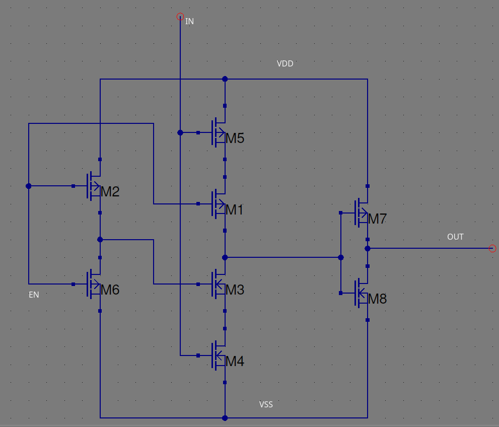
The schematics below which has been drawn in Qucs, can be found in the LibrePDK GitLab repo and shows a driver with an input, output and enable signal.
Converting the netlist into JSON results in the file which can be found in the GitLab repo as well
It’s 8 transistors with M7/M8 being the output stage which have to drive all the current and hence need a muss lower on resistance respectively saturation current.
{
	"name": "driver_circuit",
	"nets": ["VDD","VSS","EN","IN","OUT"],
	"instances": {
		"M1": {
			"type":"pmos",
			"nets": {
				"drain": "3",
				"gate": "EN",
				"source": "4",
				"bulk": "4"
			},
			"R_on": 1000.0,
			"V_DS": 1.2
		},
		"M2": {
			"type":"pmos",
			"nets": {
				"drain": "1",
				"gate": "EN",
				"source": "VDD",
				"bulk": "VDD"
			},
			"R_on": 1000.0,
			"V_DS": 1.2
		},
		"M3": {
			"type":"nmos",
			"nets": {
				"drain": "3",
				"gate": "1",
				"source": "2",
				"bulk": "2"
			},
			"R_on": 1000.0,
			"V_DS": 1.2
		},
		"M4": {
			"type":"nmos",
			"nets": {
				"drain": "2",
				"gate": "IN",
				"source": "VSS",
				"bulk": "VSS"
			},
			"R_on": 1900.0,
			"V_DS": 1.2
		},
		"M5": {
			"type":"pmos",
			"nets": {
				"drain": "4",
				"gate": "IN",
				"source": "VDD",
				"bulk": "VDD"
			},
			"R_on": 1000.0,
			"V_DS": 1.2
		},
		"M6": {
			"type":"nmos",
			"nets": {
				"drain": "1",
				"gate": "EN",
				"source": "VSS",
				"bulk": "VSS"
			},
			"R_on": 1000.0,
			"V_DS": 1.2
		},
		"M7": {
			"type":"pmos",
			"nets": {
				"drain": "OUT",
				"gate": "3",
				"source": "VDD",
				"bulk": "VDD"
			},
			"R_on": 100.0,
			"V_DS": 1.2
		},
		"M8": {
			"type":"nmos",
			"nets": {
				"drain": "OUT",
				"gate": "3",
				"source": "VSS",
				"bulk": "VSS"
			},
			"R_on": 100.0,
			"V_DS": 1.2
		}
	}
}
Lets say we’ve cloned the repo with
git clone https://gitlab.libresilicon.com/generator-tools/librepdk.git
cd librepdk
export LIBREPDK_REPO=`pwd`
Running that JSON file through LibrePDK with the command below leaves us not only with a GDSII but also a SPICE model, Magic VLSI, DEF and LEF file.
export DESIGN_DIR=$LIBREPDK_REPO/tests/driver_circuit
export DESIGN_FILE=$DESIGN_DIR/driver_circuit.json
export ANAROUTE_WORKDIR=$LIBREPDK_REPO/workdir_driver
export ANAROUTE_DEBUG_OUT=$ANAROUTE_WORKDIR/debug/
export ANAROUTE_DEBUG_OUT_PREFIX=$ANAROUTE_DEBUG_OUT/snapshot
rm -rf $ANAROUTE_WORKDIR
mkdir -p $ANAROUTE_DEBUG_OUT
pushd $ANAROUTE_WORKDIR
uv run ../bin/librepdk_generator -d $DESIGN_FILE -t SG13G2 -o out &> out.log
cp $DESIGN_DIR/*.spice .
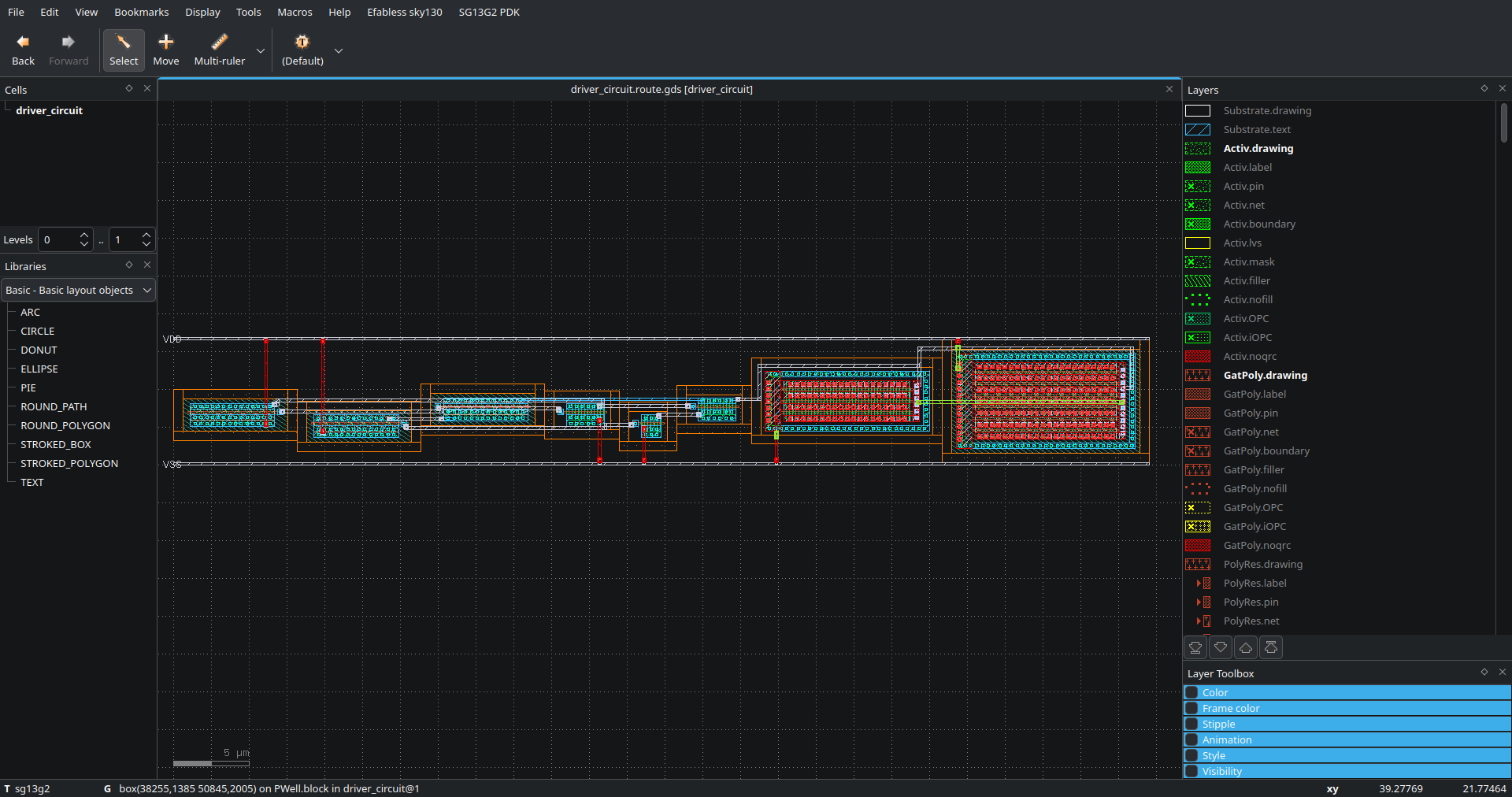
popdFirst lets look at the GDS2 file. We can easily identify M7 and M8 because they’re much larger than the other transistors and have fingers.
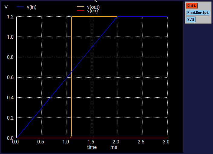
Running the test simulations in NG Spice for when the input is enabled and disabled results in the desired behavior.
Output enable is inverted so when it’s 1 (VDD) the output is disabled, when it’s 0 (VSS), the output is enabled.
The below NGSPice simulation shows the result of running `ngspice workdir_driver/test1.spice with the output being disabled.
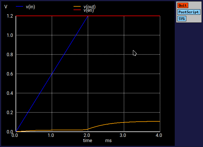
The below NGSPice simulation shows the result of running `ngspice workdir_driver/test2.spice with the output being enabled.